"Insulation" & "Mad Soldering 5k!|z"
The prototypes just keep comin' in.
They arrive in the form of boards with components freshly placed on them via the SMT process. Part of my job was to build them into "Stealth" units, which conceals the actual final cosmetic outlook of the unit by containing the prototype in a bare-bones casing.
It isn't difficult, albeit this being my first time, and I had only 4 units to build. So I was merrily following the directions and putting on heatsinks and driving screws, when my boss came around and said:
"You forgot to put the tape around the big chips."
I was like, "Huh?" And he pointed out the following to me.
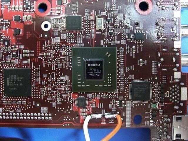 |
Figure 1: nVidia GPU (Graphics Processing Unit) and unprotected on-chip components.
To put it simply, the green square with the sprinkles of rectangles and the reflective center chip, that whole thing, is the nVidia GPU of our new prototype. Unfortunately, I do not have a picture that shows how the height of the little grains of rectangles (resistors and capacitors) are actually the same height as the central reflective square (the chip's die).
Check out the following picture.
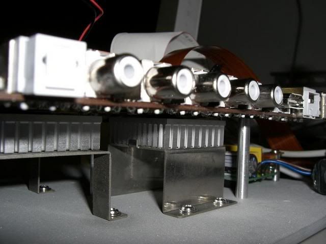 |
Figure 2: Side view of the nVidia chip with heatsink attached.
The heatsink is the grey thing in the middle of the picture with the fingers sticking downwards. There is double-sided tape between the bottom of the heatsink and the GPU's die, holding the heatsink in place.
If you can make it out, there is very little clearance between the flat part (the bottom) of the heatsink and the packaging (the green part) of the GPU. Any little bit of tilting of the heatsink would cause it to connect with the resistors and capacitors on the packaging, causing shorts which could hang the system at best and be a system-level catastrophy at the worst.
So this was what my boss suggested to do.
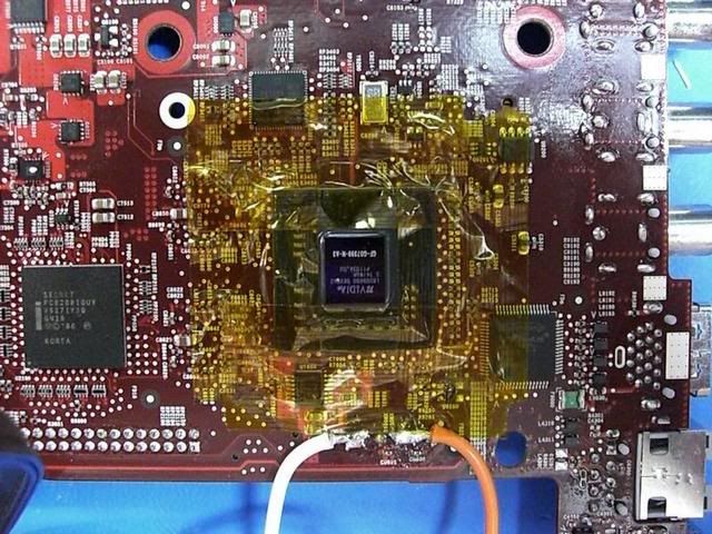 |
Figure 3: nVidia chip with its on-chip components protected by Kapton tape.
I wanted to put this down because I think this was an important lesson. In manufacturing, boards are handled by people all the time, especially during testing when the boards are bare and there is no casing. In these situations, it is very easy to accidentally tilt the heatsink, and thereby cause a short if there were nothing insulating the components. I gotta try and think this way in the future, try to consider all the conceivable sources of dangers. And not just in the immediate time frame and place, but far down the line, too!
I was asked to solder on a few clock crystals this afternoon which were first desoldered from other boards. First of all, this was how the result looked, done via the SMT process:
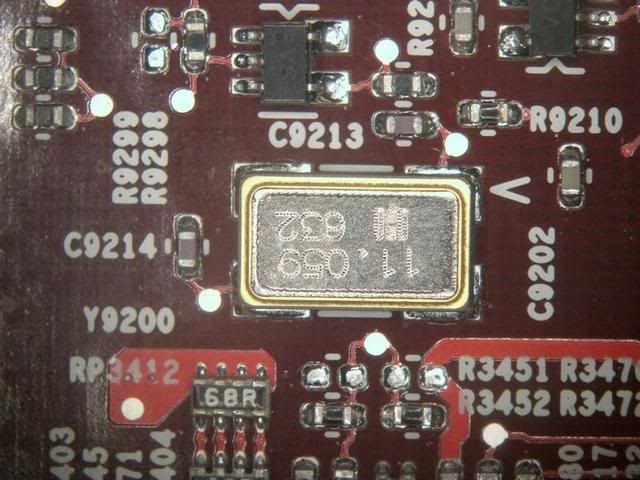 |
Figure 4: SMT-soldered clock crystal.
Now, of course, this was done by a machine (a few, in fact), and a human being could never hope to match the precision. But, what I did was... atrocious:
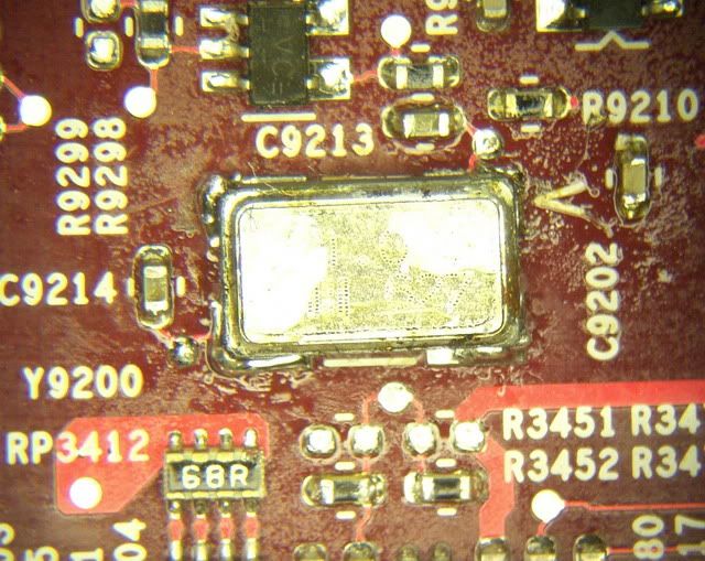 |
Figure 4: The crystal soldered by yours truly.
(Picture forthcoming)
Clearly, I have a lot to learn even about basic skills like soldering. Everything worked fine, despite my best efforts. But what I learned was this.
The first thing to do is to make sure that all the contact pads for the crystal on the board are flat. This means removing any solder already on the pads. Then, you solder one contact corner of the crystal onto the correct corresponding pad on the board and watch the placement!!!
If the part is placed correctly, centered and all, then there would be enough of the pads exposed that any application of flux and then solder would cause the solder to be sucked right onto the metal, making the hand-soldering process really simple.
By the way, here's a size comparison with a dime.
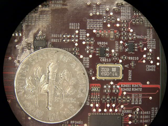 |
Figure 5: Size comparison of a dime and the clock crystal.
This is something to keep in mind, especially since I am supposed to help our customer's R&D team in doing tests and measurements and whatnot, which would require this skill.
Besides, it's fun! :)
posted by Grasshopper Engineer at 12:56 AM
![]()

0 Comments:
Post a Comment
<< Home