Overdesign of Overcurrent Protection?
(Preface: To tell you the truth, the previous two entries were actually written nearly a week ago, on another diary site. I had wanted to move them over here sooner, but only yesterday did that other diary site come back online and I was able to grab the entry from there. In other words, it's been a few days since the last entry and this one.)
As more and more boards come in, we're discovering a seemingly endless stream of issues that need to be confronted and resolved before the next stage of development is possible. One of the most persistent and obstructive is the +1.5V and +1.2V power supply.
The issue is the following list of symptoms from my diagnosis.
(NOTE: On different boards, it measures out to different values, but all the malfunctioning boards have this voltage measuring out to be within the range of +0.6V to +0.8V. The same thing would happen with the +1.2V voltage -- it would measure out to be around half of its intended level.)
These voltages power vital components on the system:
We found no apparent issues with the circuit design of those areas. Below is the schematic for the power circuitry for the +1.5V power rail.
Figure 1: The +1.5V Power Supply Circuit Schematic.
Over the course of a week or so, the Power engineer from our customer (our own Power engineer was busy with another project) did his own investigation and found that the following possible causes.
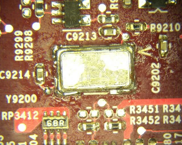
Figure 2: Bulk Capacitors for the Northbridge. You can tell that the power line (=PP1V5_S0_NB_3G) is going to the Northbridge by the "NB" circled in green.
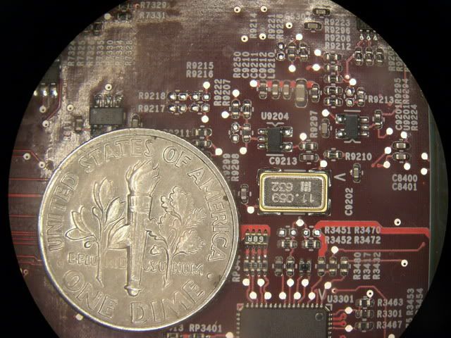
Figure 3: Bulk Capacitors for the Southbridge. You can tell that the power line (=PP1V5_S0_SB) is going to the Southbridge by the "SB" circled in green.
Notice the bulk capacitors (220uF) in both screenshots. Their purpose in this case is to store a lot of energy. When the machine is operating, if for some reason the ICs (NB or SB) suddenly need a large surge of energy, they can get it from these capacitors instead of drawing too much too quickly from the power ICs themselves (such as the Uxx00) that they overheat and burn out.
But these protective devices are causing problems, too. During boot-up, because these are initially empty, the demand for current really is that great. The power IC is supposed to be able to handle this kind of punishment for a while, but apparently they are not. So this is what's happening:
This is why the voltage output from the power ICs is always a fraction of their correct values. Just to confirm it, I put in a 1-Ohm resistor in series with the Inductor L7800 at pin 1 on a problematic board. The problem went away immediately. I've attached a photo of it below.
Figure 4: The 1-Ohm Current-Limiting Resistor Experiment.
This is how it looked before:
Figure 5: Before the 1-Ohm Current-Limiting Resistor Experiment.
You could say that my soldering/rework skills have improved, eh? :D
So in any case, the current work-around for this stage in Prototyping is to unstuff those bulk capacitors (for the +1.5V issue; for the +1.2V and +3.3V there are similar solutions), to remove them before testing them. The 1-Ohm Resistor insertion rework takes longer to do than to simply remove the capacitors.
After working with the makers of the power ICs, it was found that the power IC itself is not "ignoring" the overcurrent condition for long enough at startup. What this means is that the power IC is supposed to just go ahead and supply that large current for some time until the bulk capacitors fill up and the system becomes stable, but it wasn't supplying that large current for long enough before thinking that danger is happening. So the power IC company has promised to adjust their ICs so that in a future version, the time before shutdown is longer. This version would be in full production only after the next phase of our developmen.
Our customer has decided, however, that that would be much too long to wait, so their Power engineer has found another usable power IC from another company.
So was this an overdesign of overcurrent protection? I don't know, because perhaps the system would never need that much current anyway. What I learned from this experience, though, is to always look beyond the immediate region of where the problem is supposed to occur, and investigate all the points where this region touches. I believe that if I had done that, I would have easily been the one to discover those bulk capacitors and helped solve the problem that much more quickly.
As more and more boards come in, we're discovering a seemingly endless stream of issues that need to be confronted and resolved before the next stage of development is possible. One of the most persistent and obstructive is the +1.5V and +1.2V power supply.
The issue is the following list of symptoms from my diagnosis.
- System No Boot.
- ALL_SYS_PWRGD (All Systems Power Good) LED shows power malfunction.
- +1.5V power rail measures to be just under 1/2 of correct value.
- Power-On Sequence signals up to that point are all normal.
(NOTE: On different boards, it measures out to different values, but all the malfunctioning boards have this voltage measuring out to be within the range of +0.6V to +0.8V. The same thing would happen with the +1.2V voltage -- it would measure out to be around half of its intended level.)
These voltages power vital components on the system:
- Parts of the CPU
- Parts of the Southbridge
- Parts of the Northbridge
- Wireless Ethernet
- PCIE
- the Graphics Processor
We found no apparent issues with the circuit design of those areas. Below is the schematic for the power circuitry for the +1.5V power rail.
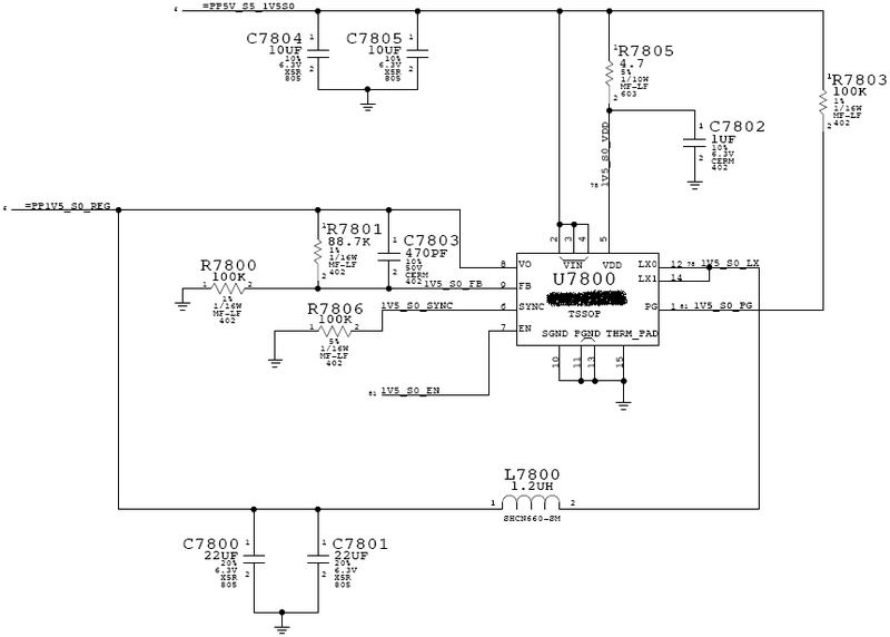 |
Figure 1: The +1.5V Power Supply Circuit Schematic.
Over the course of a week or so, the Power engineer from our customer (our own Power engineer was busy with another project) did his own investigation and found that the following possible causes.
 |
Figure 2: Bulk Capacitors for the Northbridge. You can tell that the power line (=PP1V5_S0_NB_3G) is going to the Northbridge by the "NB" circled in green.
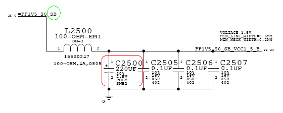 |
Figure 3: Bulk Capacitors for the Southbridge. You can tell that the power line (=PP1V5_S0_SB) is going to the Southbridge by the "SB" circled in green.
Notice the bulk capacitors (220uF) in both screenshots. Their purpose in this case is to store a lot of energy. When the machine is operating, if for some reason the ICs (NB or SB) suddenly need a large surge of energy, they can get it from these capacitors instead of drawing too much too quickly from the power ICs themselves (such as the Uxx00) that they overheat and burn out.
But these protective devices are causing problems, too. During boot-up, because these are initially empty, the demand for current really is that great. The power IC is supposed to be able to handle this kind of punishment for a while, but apparently they are not. So this is what's happening:
- The power ICs are forced to supply a large amount of current, which they detect that they don't want to handle.
- The power ICs shut themselves off because they think that if they kept going, it'd get a bit toasty.
- The Northbridge and Southbridge drain the previously somewhat-charged bulk capacitances of their stored power.
- The power ICs finally wake up, and sees that they need to get to work. Go back to Step 1.
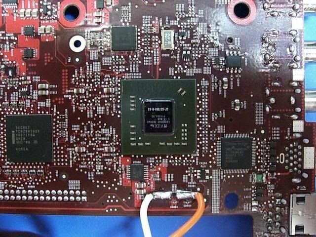
This is why the voltage output from the power ICs is always a fraction of their correct values. Just to confirm it, I put in a 1-Ohm resistor in series with the Inductor L7800 at pin 1 on a problematic board. The problem went away immediately. I've attached a photo of it below.
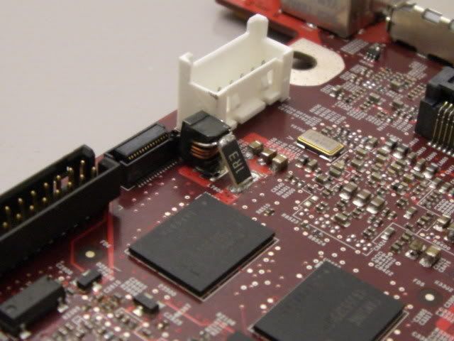 |
Figure 4: The 1-Ohm Current-Limiting Resistor Experiment.
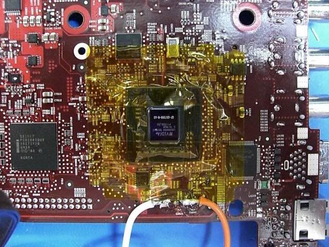
This is how it looked before:
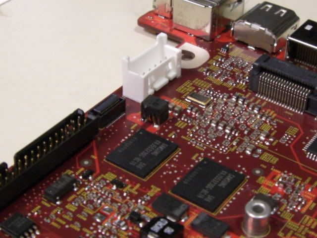 |
Figure 5: Before the 1-Ohm Current-Limiting Resistor Experiment.
You could say that my soldering/rework skills have improved, eh? :D
So in any case, the current work-around for this stage in Prototyping is to unstuff those bulk capacitors (for the +1.5V issue; for the +1.2V and +3.3V there are similar solutions), to remove them before testing them. The 1-Ohm Resistor insertion rework takes longer to do than to simply remove the capacitors.
After working with the makers of the power ICs, it was found that the power IC itself is not "ignoring" the overcurrent condition for long enough at startup. What this means is that the power IC is supposed to just go ahead and supply that large current for some time until the bulk capacitors fill up and the system becomes stable, but it wasn't supplying that large current for long enough before thinking that danger is happening. So the power IC company has promised to adjust their ICs so that in a future version, the time before shutdown is longer. This version would be in full production only after the next phase of our developmen.
Our customer has decided, however, that that would be much too long to wait, so their Power engineer has found another usable power IC from another company.
So was this an overdesign of overcurrent protection? I don't know, because perhaps the system would never need that much current anyway. What I learned from this experience, though, is to always look beyond the immediate region of where the problem is supposed to occur, and investigate all the points where this region touches. I believe that if I had done that, I would have easily been the one to discover those bulk capacitors and helped solve the problem that much more quickly.
posted by Grasshopper Engineer at 5:04 PM
0 comments
![]()